


The Zhitong Finance App learned that as artificial intelligence (AI) models evolve from training to advanced reasoning and intelligence (Agentic AI), the focus of infrastructure is quietly shifting from “computational power dominance” to “memory dominance.”
Facing the increasingly expensive “memory wall (memory wall),” Bernstein, a well-known investment bank, pointed out in a newly released in-depth research report that high-bandwidth flash memory (HBF, High Bandwidth Flash) is expected to be the key to breaking the game. Not only is this technology expected to drastically reduce AI inference costs, but it is also likely to have a reshaping effect similar to HBM on the DRAM industry for the NAND industry, which is mired in a cycle quagmire.
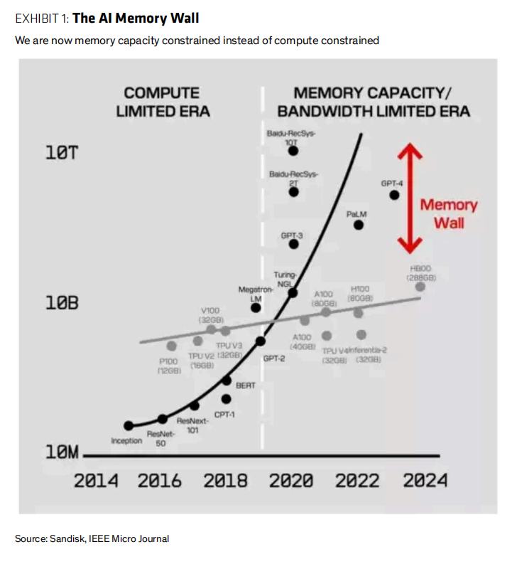
The evolution of AI has spawned a “memory wall”, where reasoning and intelligence consume large computing power
Bernstein notes in his report that iterations of AI technology are reshaping underlying hardware requirements. In the training phase, GPUs and HBM (high-bandwidth memory) occupy a central position; however, with the exponential expansion of large language model parameters, the continuous lengthening of the context window (approaching or exceeding 1 million tokens), and the urgent need of agents for long-lasting interaction, massive data has far exceeded the economic capacity boundary of HBM, and is gradually spilling over into traditional DRAM, NAND flash memory, and a wider range of storage tiers such as HDD and tape.
Analyst Mark C. Newman and his team emphasized in the report that the inference process, especially the decoding phase, is a typical “limited memory bandwidth” scenario.
Under the hybrid expert model (MoE) architecture, even though only some experts are activated in a single inference, a huge total set of parameters must be on standby at any time. Furthermore, the cache mechanism (KV Cache) has created a huge economic incentive — currently mainstream AI labs and Google only read the cache token at about 10% of the new input token.
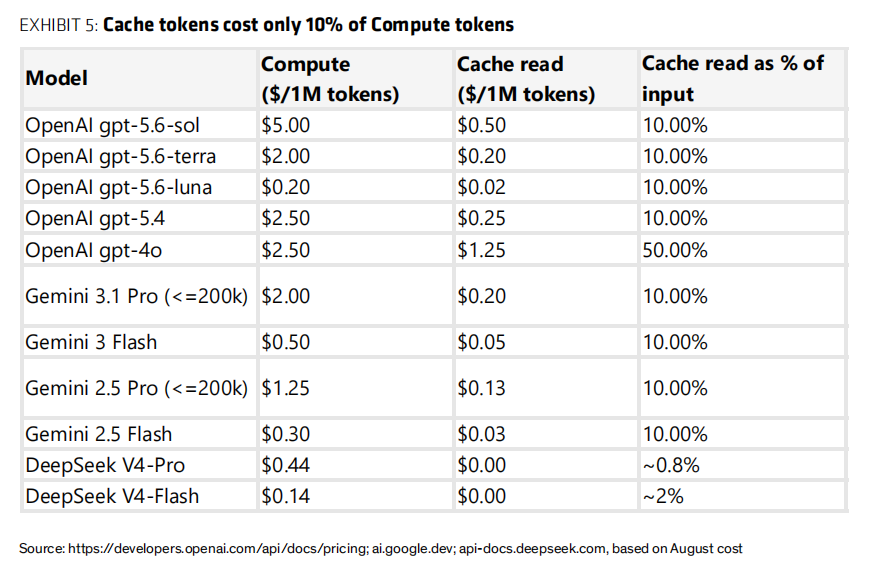
This means that in order to avoid expensive repeated computations, the system requires more capacity and higher bandwidth memory to store and reuse previous contexts. Simply increasing computing power has made it difficult to improve system utilization; memory capacity and bandwidth are becoming core bottlenecks limiting AI development.
The HBF architecture came out of nowhere: taking into account HBM bandwidth and 8-16 times the capacity
To overcome this “memory wall,” HBF technology came into being. It stacks NAND flash memory through a highly parallel, wide-interface architecture, and is designed to provide read bandwidth close to HBM, while achieving a capacity span of 8 to 16 times, and the cost per GB is significantly lower than HBM.
In the HBM+HBF hierarchical architecture proposed by SanDisk (SNDK.US), the HBM, which has a smaller capacity and extremely low latency, continues to be a “high-speed cache” for processing the most active working sets, while the HBF acts as a “capacity layer” to store massive model parameters (such as inactive experts in the MoE architecture) and warm/cold KV cache data. The H3 architecture previously proposed by SK Hynix (SKHY.US) also confirms this idea.
The economic benefits of this structure are remarkable. SanDisk's simulation tests (based on the Qwen3-480B-A35B model) showed that in a pure HBF configuration, only 1 GPU is needed to run the 960GB bFloat16 model, while the pure HBM solution requires at least 8 GPUs. The performance of 4 HBF GPUs is comparable to 8 HBM GPUs, even in scenarios where the same token needs to be output.
By drastically reducing reliance on expensive GPUs and HBM, HBF not only reduced the cost of memory per GB, but also optimized capital expenditure (CapEx) and power consumption at the system level, achieving an architecture-level leap forward in “avoiding repeated computation.”
The wafer consumption ratio is as high as 6.5 times, yet the gross margin is comparable to HBM
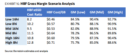
From an economic perspective, HBF's profit-boosting effect on the NAND industry chain is highly imaginative. Since it uses high-performance, high-durability SLC (single-layer unit) flash memory and requires an additional silicon area to accommodate TSV (silicon holes) and peripheral circuits, Bernstein measured the HBF's wafer consumption ratio (Trade Ratio) as high as 6.5 times, far higher than HBM; its manufacturing cost ratio is about 10 times that of enterprise-grade SSDs (eSSD).
However, thanks to its extremely high premium capacity, if HBF is priced at a module price similar to HBM (but provides 8-16 times the capacity), its gross margin can be expected to reach an astonishing 80%-90%, which is basically the same as the current NAND industry's top profit level, and greatly increases revenue and profits.
According to the report's benchmark estimates, the gross margin centers of 8-hi and 16-hi HBF modules will reach 86.5% and 88.9%, respectively, according to HBM ASP (average selling price) expectations in 2027.
Reshaping the NAND supply and demand landscape: Similar to HBM's “Jevens Paradox” for DRAM
The popularity of HBF is expected to bring structural benefits to the NAND industry similar to HBM to the DRAM industry. On the one hand, a wafer consumption ratio of up to 6.5 times means that even if HBF only accounts for 10% to 20% of the mobility rate, it will cause the industry's wafer demand to surge by 20%-120%. In the current context of slow expansion of fab production and huge capital expenditure, this will greatly tighten NAND's supply-demand balance and support prices and profit margins.
On the other hand, HBF has created new AI-driven requirements, breaking the traditional enterprise-grade SSD inventory game.
The market is generally concerned that HBF will erode HBM's demand, but Bernstein believes the two are more complementary. Although HBF reduces the HBM capacity required to store model parameters, it cannot replace HBM for active computation and token generation.
Lower AI inference costs will accelerate the spread of AI applications. According to the “Jevens Paradox,” an increase in overall efficiency may instead stimulate larger AI deployments, thereby driving the total demand for HBM, GPU, and NAND to grow exponentially.
Ecological Gaming and Landing Challenges: Nvidia's Absence and SanDisk's Ambition
Despite the broad prospects, the full commercialization of HBF still faces structural limitations and ecological challenges. Since the bottom layer is still NAND, HBF's reading latency is at the microsecond level, which cannot reach the nanosecond level of DRAM; its writing performance and durability are also limited. Therefore, HBF is more suitable for inference scenarios where you read more and write less.
The more central challenge is ecological support. Currently, the HBF Alliance has absorbed giants such as SanDisk, SK Hynix, Google (GOOGL.US), Meta (META.US), and Tensorrent, but the industry trend vane Nvidia has yet to clearly endorse it. Instead, Nvidia (NVDA.US) is actively promoting its CMX (content memory storage) platform and the Storage Next solution. Furthermore, TSM.US has yet to disclose its Advanced Packaging (CoWoS) production capacity plan for HBF.
As the core driver of HBF, SanDisk is making every effort to promote the implementation of HBF by leveraging its vertical integration advantages in NAND IP, front-end manufacturing (joint venture with Kioxia), and system-level packaging. According to reports, SanDisk's first-generation HBF product has been successfully streamed, and plans to launch the first batch of inference oriented samples in 2027, while the second-generation product will target 100 billion parameter-level models in the field of edge computing.
Taken together, HBF provides an extremely cost-effective evolutionary path to break the AI memory wall. Although the future is still constrained by shortcomings in delays and the ecological choices of major manufacturers such as Nvidia, once implemented on a large scale, it will undoubtedly inject strong structural growth momentum into the NAND industry and open up the “HBF era” of the storage industry.